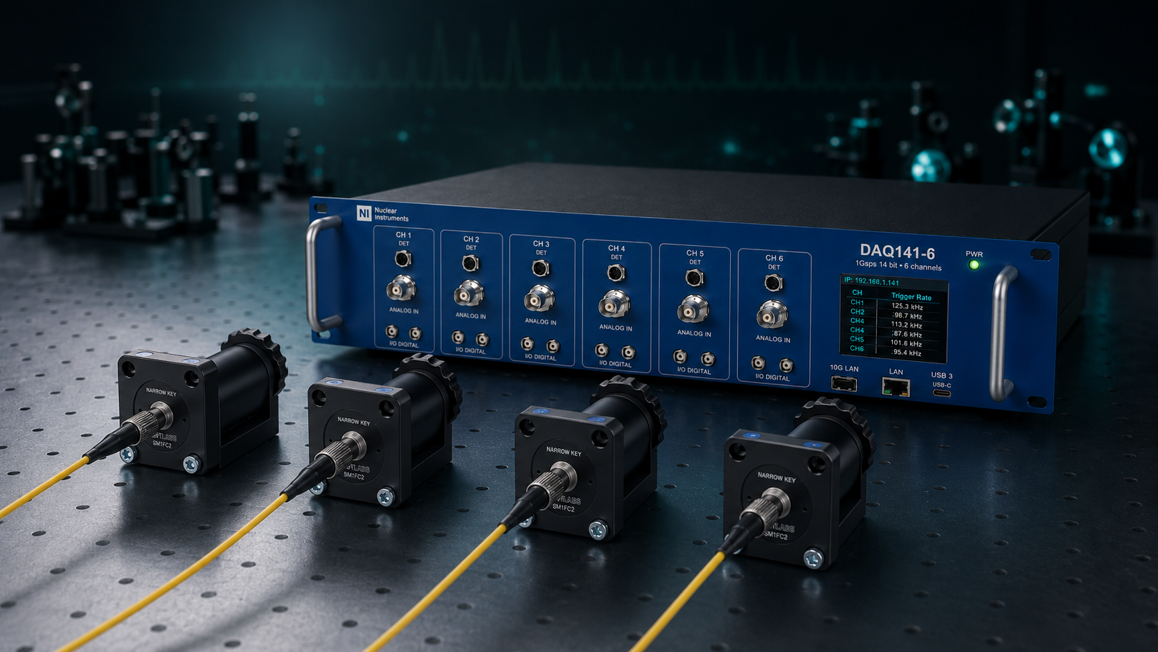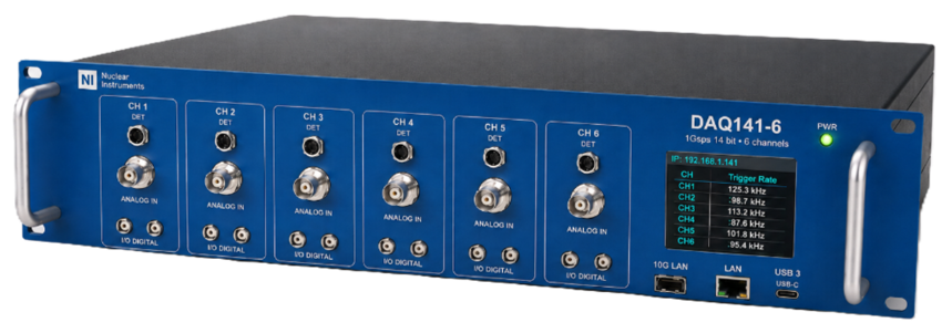

DAQ-141-6 – 6-Channel 14-bit 1 Gsps Waveform Digitizer
The DAQ-141-6 is a high-performance, 6-channel waveform digitizer developed by Nuclear Instruments for demanding scientific and industrial data acquisition. It integrates 6 independent 14-bit, 1 Gsps analog-to-digital converters with a fully programmable FPGA-based processing pipeline, on-board ARM64 computing, and flexible network output — all in a single 4U rack-mount chassis.
Each channel features a fully differential 1 GHz bandwidth front-end, a deep acquisition memory (up to 200 µs per channel), and a programmable digital processing chain. Signal data can be streamed as raw waveforms or as processed event lists via standard network protocols (Kafka, ZeroMQ), making the DAQ-141-6 a self-contained DAQ node that requires no intermediate host PC.
More than a digitizer — the heart of QuantumBox. The DAQ-141-6 belongs to the Nuclear Instruments DAQ-1×1 digitizer family, and at the same time it is the crucial building block of the upcoming QuantumBox system — our forthcoming single-photon counting product. Loaded with the QuantumBox firmware and paired with the QMPD SiPM sensor heads, the very same hardware becomes a real-time, single-photon-resolving photon-number and timing processor. Buy it today as a flexible open digitizer; tomorrow it is the engine inside QuantumBox.
Key Features
- Compatible with Sci-Compiler for FPGA pipeline generation — no HDL coding
- 6 independent analog input channels
- 14-bit ADC @ 1 Gsps per channel, true simultaneous sampling
- 1 GHz analog bandwidth, ENOB 11.3 bit, SFDR > 70 dBc
- Real-time on-board DSP: CFD timing, QDC charge integration, PHA
- Single-photon resolution with QuantumBox firmware + QMPD SiPM head
- Embedded Linux on Zynq UltraScale+ 7EV SoC (ARM64 + FPGA) — no host PC required
- 10 GbE raw-UDP and 1 GbE Kafka/ZeroMQ streaming, list-mode or waveform
- Drives 6 front-end heads: programmable bias, ±6 V, TEC, temperature feedback
- SDK (Python / C++ / C# / LabVIEW) + EPICS slow control
- WaveFLOW DAQ oscilloscope software with live scope & histograms
System Architecture
The DAQ-141-6 is built around DAQ boards, each hosting a Zynq UltraScale+ 7EV SoC module (Ultrazed) with 4 GB DDR4 and 8 GB NAND flash:
- The FPGA Programmable Logic (PL) implements the JESD204B receiver for the dual-channel ADC9680-1000 converters (14-bit, 1 Gsps), the acquisition pipeline, pre-trigger FIFO, DMA engine, and digital processing cores
- The ARM Processing System (PS) runs embedded Linux and handles network I/O, Kafka/ZeroMQ clients, the EPICS IOC, and custom user algorithms
- Each ADC9680-1000 provides a 4-lane JESD204B interface at 12.5 Gbps
- A low-jitter, temperature-compensated clock generator supplies the 1 GHz ADC clock and the 250 MHz FPGA fabric clock, with selectable source: on-board TCXO or external clock
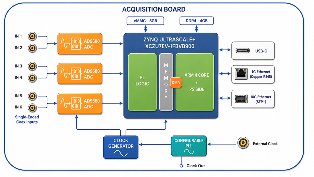
DAQ board block diagram: JESD204B interface, Zynq UltraScale+ SoC, DDR4, and Ethernet output.
DAQ board block diagram: JESD204B interface, Zynq UltraScale+ SoC, DDR4, and Ethernet output.
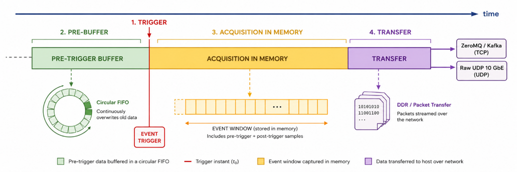
On-board firmware pipeline — acquisition, pre-trigger FIFO, and reconfigurable digital processing cores.
On-board firmware pipeline — acquisition, pre-trigger FIFO, and reconfigurable digital processing cores.
Two Operating Modes
The same hardware platform operates in two complementary modes, so it can be adapted to photon detection, nuclear instrumentation, spectroscopy, time-of-flight, beam diagnostics, detector readout, and fast transient analysis.
Digitizer Mode
A multi-channel waveform recorder. On a trigger, all channels are acquired simultaneously; a programmable pre-trigger region is preserved from the internal circular buffer while the post-trigger waveform is stored until the acquisition window completes. Full waveforms are transferred over the network via ZeroMQ/Kafka, or streamed as raw UDP over the 10 GbE interface for maximum throughput. Ideal for offline analysis, algorithm development, detector characterization, and ML dataset generation.
Processor Mode
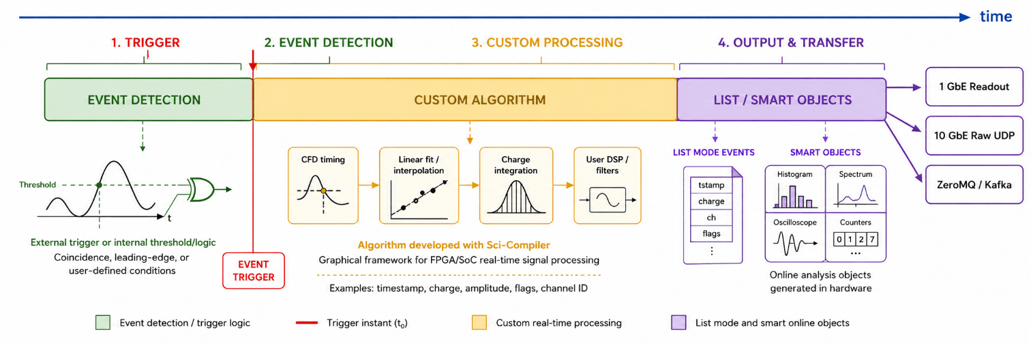
Real-time event detection, signal analysis, and data reduction directly on the embedded FPGA/SoC. A configurable trigger stage (threshold, coincidence, timing condition) identifies events, then a custom processing algorithm runs in real time. Output can be transferred in compact list mode — each event represented by timestamp, amplitude, charge, channel ID, flags or user-defined quantities — while the firmware simultaneously generates online histograms, spectra, rate meters, and diagnostic counters. Custom blocks (filters, discriminators, integrators, counters, histogrammers, timing extractors, coincidence logic, event builders) are built with Sci-Compiler, without writing the complete HDL design.
QuantumBox — Single-Photon Processing
When the same platform is configured as QuantumBox, the processor firmware is optimized for SiPM-based photon detection, time-tagging, and charge measurement:
- The trigger is provided externally (e.g. a laser synchronization signal) or internally by a leading-edge threshold on the detector signal
- A digital Constant Fraction Discrimination algorithm extracts the event time; a linear regression around the CFD crossing interpolates the timestamp with timing resolution down to 50 ps
- Programmable charge integration (QDC) runs simultaneously on all channels
- Event data are formatted as a compact list (timestamp, integrated charge, channel) and streamed over 1 GbE or, for higher rates, 10 GbE raw UDP
- In parallel the FPGA accumulates real-time per-channel spectra for online monitoring of the photon-number distribution, signal stability, and detector response
This is exactly the 1 Gsps, 14-bit real-time chain — QDC processing, event-list output, 50 ps time tagging, real-time spectra and 10 GbE streaming — that the QuantumBox product is built upon.
QuantumBox firmware: CFD timing, QDC charge integration, and real-time photon-number spectra running on the DAQ-141-6 FPGA.
QuantumBox firmware: CFD timing, QDC charge integration, and real-time photon-number spectra running on the DAQ-141-6 FPGA.
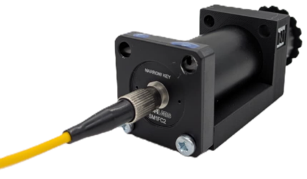
QMPD sensor module — 1.3 × 1.3 mm² SiPM with variable-gain transimpedance preamplifier and on-board temperature monitor.
QMPD sensor module — 1.3 × 1.3 mm² SiPM with variable-gain transimpedance preamplifier and on-board temperature monitor.
Phase-Locked Acquisition
The DAQ-141-6 is designed to operate in phase lock with a coherent light source, so the integration window always begins in a fixed, repeatable phase relationship with the instant of laser emission, reducing the aperture jitter to a few picoseconds:
- Digitizer as master: the
CLOCK OUToutput delivers any sub-multiple of the internal 1 GHz sampling frequency, providing a clean, low-jitter reference that drives the laser while remaining inherently phase-locked to the ADC sampling clock - Laser as master: a programmable PLL accepts an external reference (from the laser oscillator or a monitor photodiode), multiplies it up to 1 GHz, and uses the result as the sampling clock so the digitizer follows the optical emission
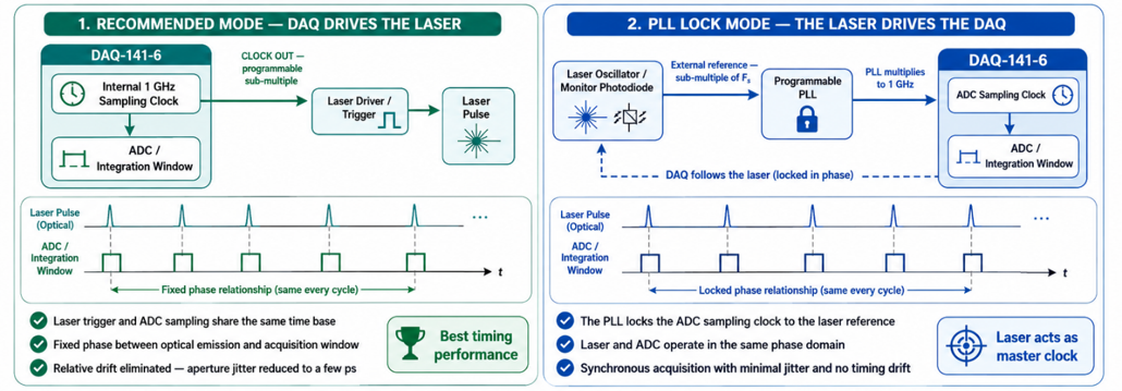
Phase-locked operation: laser trigger and sampling clock derived from the same time base, eliminating relative timing drift between excitation and acquisition.
Phase-locked operation: laser trigger and sampling clock derived from the same time base, eliminating relative timing drift between excitation and acquisition.
Front-End Power & Control
The DAQ-141-6 can power and control up to six front-end boards. Nuclear Instruments currently supplies the QMPD module — a 1.3 × 1.3 mm² SiPM with a variable-gain transimpedance preamplifier (dynamic range selectable between 10 p.e. and 200 p.e.) and an on-board temperature monitor for active gain/bias compensation. Each head connects through a single M8 connector on the front panel, directly above its analog channel, providing:
- Programmable BIAS for the SiPM, up to 80 V at 10 mA, with low output noise
- Ultra-low-noise ±6 V supply at 500 mA for the preamplifier and analog electronics
- 24 V supply at 500 mA for the Peltier (TEC) cooling element
- Analog temperature feedback (0–3.3 V) sampled by a dedicated 16-bit ADC
- One-wire connection to read the calibration EEPROM and monitor the preamplifier board temperature
WaveFLOW DAQ Software
WaveFLOW is the dedicated PC-side acquisition and visualization software for the DAQ-141-6, with a professional oscilloscope interface, real-time measurement panels, histogram views, and a complete waveform dump facility (CSV, BIN, TXT, MATLAB) in a modern dark-themed GUI. It connects to one or more DAQ-141-6 over the network and streams live waveforms in a multi-trace scope view, exposing every key digitizer parameter — trigger mode, self-coincidence (OR / AND / majority), polarity, inhibit window, acquisition window, and per-channel offset and threshold — in real time.
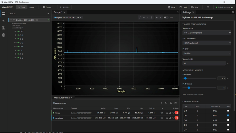
WaveFLOW multi-trace oscilloscope view with per-channel trigger configuration.
WaveFLOW multi-trace oscilloscope view with per-channel trigger configuration.
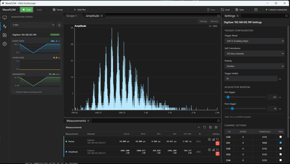
Real-time histogramming and measurement panels for online monitoring.
Real-time histogramming and measurement panels for online monitoring.
I/O & Connectivity
- 12 TTL LEMO I/O (6 IN + 6 OUT), configurable direction, 1 kΩ / 50 Ω or Hi-Z input impedance
- CLOCK IN / CLOCK OUT (SMA), directly connected to the main PLL, up to 100 MHz
- USB-C 3.2 read-out port with RNDIS (Ethernet emulation) support
- 1× SFP+ optical cage on the Zynq UltraScale+ FPGA — 10 GbE UDP streaming
- 1 GbE Ethernet port per DAQ board — Kafka / ZeroMQ
- USB-JTAG for FPGA programming and debug, USB-Serial for Linux console access
Applications
- Single-photon counting and photon-number resolution (QuantumBox)
- Time-correlated and time-of-flight measurements with SiPMs
- Nuclear instrumentation and spectroscopy
- Beam diagnostics and fast transient analysis
- Custom detector readout in high-rate environments