About the Project
The Low Energy Module (LEM) is a compact, high-precision particle spectrometer developed for the NUSES satellite to detect low-energy protons and electrons in low Earth orbit. The detector employs a hybrid readout system combining silicon PIPS sensors and plastic scintillators with SiPMs, supported by a powerful onboard DAQ and FPGA firmware, enabling high-rate histogram and list mode acquisition.
-
Date
May 2025
Nuclear Instruments
GSSI - Gran Sasso Science Institute
INFN - Istituto Nazionale di Fisica Nucleare
Dipartimento di Fisica - Universitá di Trento
Gran Sasso Tech, L’Aquila
Thales Alenia Space
Sòphia High Tech S.r.l.
AGE Scientific SRL
Introduction — What is the LEM?
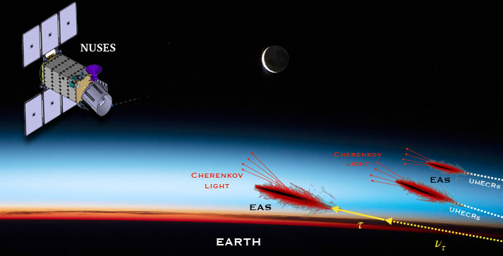
The Low Energy Module (LEM) is a compact, high-performance particle spectrometer specifically designed for operation in Low Earth Orbit (LEO) as part of the NUSES space mission. Developed in collaboration with the Nuclear Instruments team, the LEM is integrated into the Zirè payload, one of the two scientific instruments aboard NUSES, alongside Terzina, an optical telescope for Cherenkov detection.
The LEM’s mission is focused on detecting and identifying low-energy charged particles — particularly electrons in the 0.1 to 7 MeV range and protons between 3 and 50 MeV — with high precision in energy and direction. Despite its small form factor, the LEM brings to orbit a unique combination of hybrid detection, onboard digital signal processing, and real-time event classification, all within a compact 10 × 10 × 10 cm³ volume and a total mass under 2 kg.
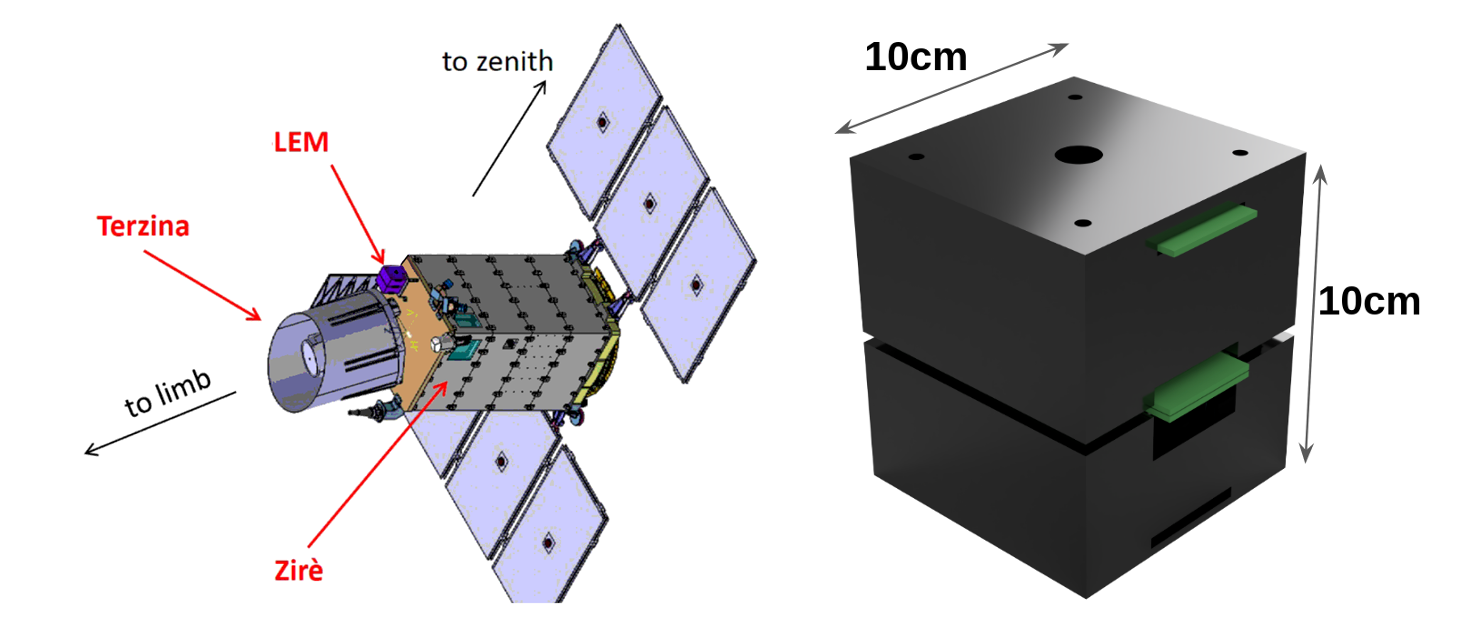
Location of the LEM detector on Nuses satellite
Location of the LEM detector on Nuses satellite
Our Contribution: DAQ Design, Firmware and System Integration
Nuclear Instruments led the complete development and qualification of the LEM data acquisition system and managed its integration as a subsystem within the NUSES satellite architecture. Our contributions include:
- Design and development of the custom DAQ boards, including digitization chain, and control circuitry
- Firmware development on Artix-7 FPGA, implementing real-time processing: trigger logic, trapezoidal filtering, histogramming, and data packetization
- Flight qualification and environmental testing of the DAQ electronics, ensuring reliable performance in space environments
- Subsystem integration of the LEM detector into the NUSES satellite, including interface definition, mechanical mounting, power/data interconnects, and protocol validation
- Coordination with consortium partners for mechanical, thermal, and electrical compatibility, ensuring seamless operation within the Zirè payload
Scientific Objectives
The LEM was conceived to address a variety of open scientific questions and space-weather monitoring needs:
- Particle precipitation from the Van Allen Belts: LEM is designed to detect Particle Bursts (PBs), sudden enhancements in electron or proton fluxes associated with geomagnetic disturbances, solar flares, or seismic activity on Earth.
- Investigation of the South Atlantic Anomaly (SAA): A particularly harsh region for space electronics, the SAA is characterized by high fluxes of trapped charged particles. LEM is built to operate reliably in this challenging environment, using active and passive shielding.
- Monitoring magnetospheric interactions: By measuring directional fluxes of low-energy particles, LEM contributes to modeling Lithosphere–Atmosphere–Ionosphere–Magnetosphere (LAIM) coupling processes.
- Seismic precursors detection: Building on previous correlations between particle bursts and large seismic events, the LEM aims to establish better statistical evidence for particle-based earthquake precursors.
- Complementary observation to Zirè: While Zirè monitors mid-to-high-energy particles, LEM extends the detection capability to lower energy channels, providing a continuous spectrum of measurements over the entire orbit.
Key Features
Despite its miniature form factor, the LEM includes:
- Five ∆E–E spectrometers for charged particle identification using stacked Passivated Implanted Planar Silicon (PIPS) detectors.
- Active collimation: Using custom-shaped plastic scintillators acting as Anti-Coincidence Detectors (ACDs) to reject scattered or off-axis particles.
- Plastic calorimeter: Extending the dynamic range up to 10 MeV for electrons.
- Dual-mode data acquisition system: Enabling both list mode (event-by-event) and histogram mode (continuous rate-based acquisition), depending on the local event rate.
- Custom-designed electronics: Including dedicated preamplifiers for both silicon detectors and SiPM-based scintillators, as well as a 16-channel digital MCA board based on the ADS52J90 ADC and Artix-7 FPGA platform.
- Redundant FPGA logic, on-board temperature sensors, and real-time housekeeping diagnostics.
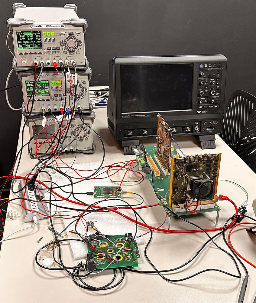
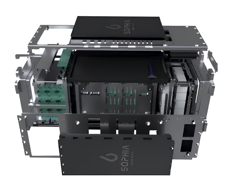
First test of readout electronics and LEM detectors in Nuclear Instruments
First test of readout electronics and LEM detectors in Nuclear Instruments
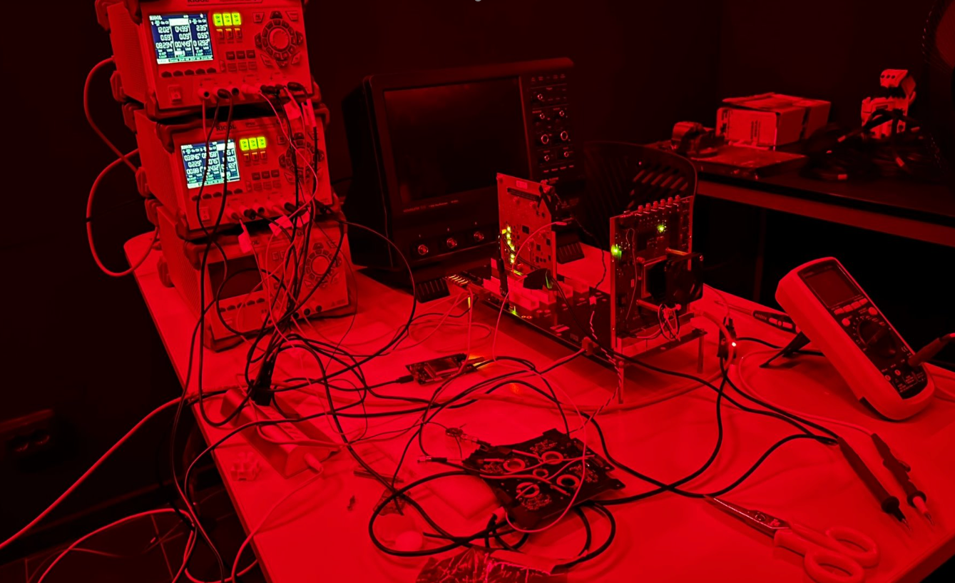
Nuclear Instruments Dark Room/EMC shilded faraday cage for SiPM and silicon detector validation
Nuclear Instruments Dark Room/EMC shilded faraday cage for SiPM and silicon detector validation
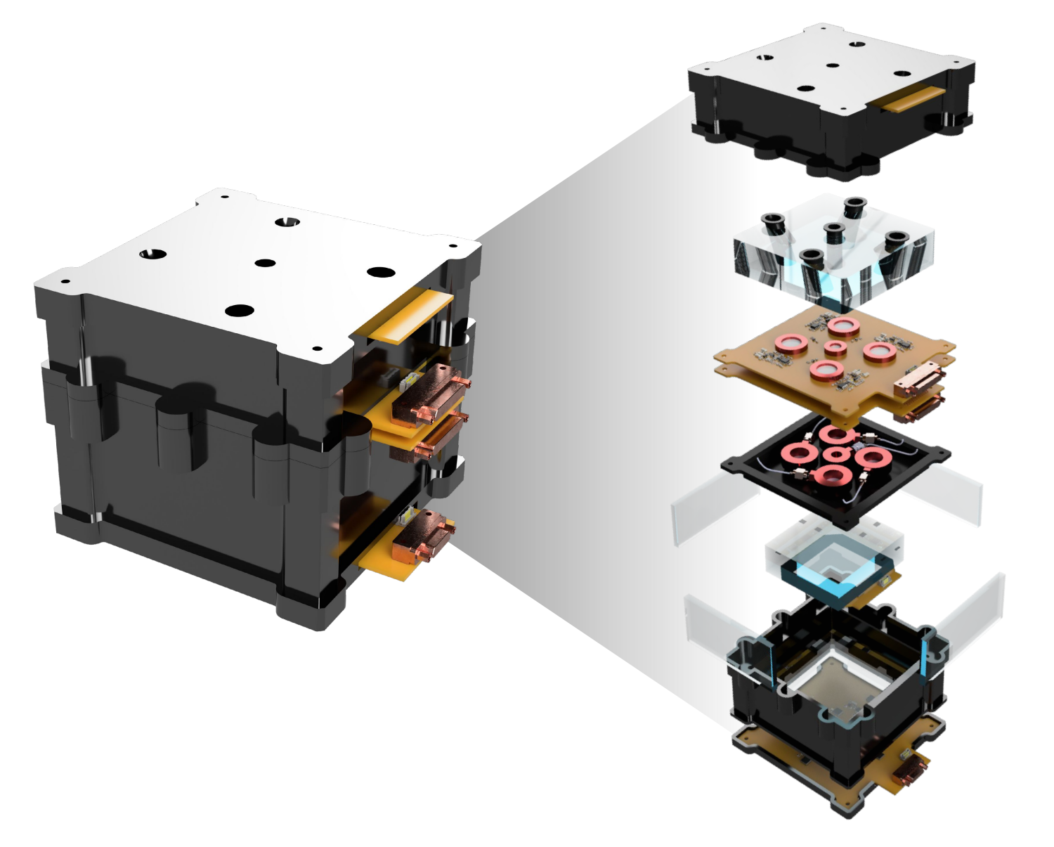
Detector Geometry and Design Philosophy
The LEM detector is built upon a layered and collimated architecture that enables both energy and directional resolution of incident particles. At its core, the LEM features a stack of custom-designed silicon detectors and plastic scintillators, configured to allow precise discrimination of charged particles based on their energy loss and penetration depth. This structural layout also supports a robust and programmable trigger logic essential for real-time classification.
Internal Structure
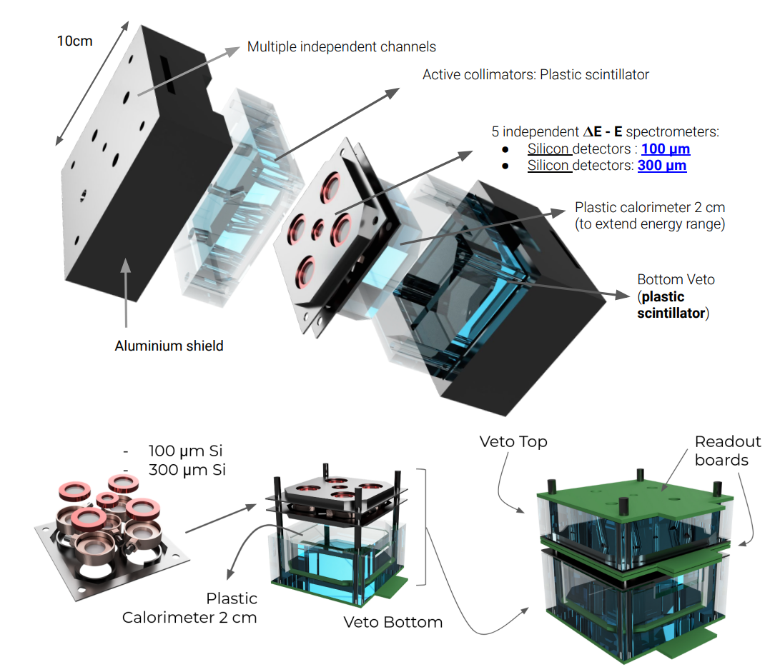
Layered structure of the LEM showing top and bottom veto scintillators (VT/VB), stacked thin and thick silicon detectors, and inner plastic calorimeter
Layered structure of the LEM showing top and bottom veto scintillators (VT/VB), stacked thin and thick silicon detectors, and inner plastic calorimeter
The LEM consists of the following principal components arranged vertically, from top to bottom:
- Veto Top (VT): An anti-coincidence shield composed of plastic scintillators read out by SiPMs, designed to reject particles entering from unwanted directions.
- Thin Silicon Layer Stack (5 detectors): These 100 µm or 300 µm PIPS detectors measure the energy loss (ΔE) of incoming particles, enabling charge discrimination and directional filtering.
- Thick Silicon Layer Stack (5 detectors): Located beneath each thin detector, the 300 µm PIPS sensors act as stopping detectors (E), allowing precise particle identification via ΔE–E methods.
- Plastic Inner (PI) Calorimeter: A plastic scintillator located beneath the silicon stack, used to extend the detection dynamic range, particularly for electrons with higher energies.
- Veto Bottom (VB): Similar to VT, this scintillator layer acts as a secondary anti-coincidence barrier, rejecting upward-going particles or scattered tracks.
Hybrid Sensor System: Silicon Detectors and SiPMs
The LEM detector adopts a hybrid architecture that combines two complementary detection technologies to achieve high energy resolution, broad dynamic range, and reliable particle identification (PID). The core sensing elements include:
- PIPS (Passivated Implanted Planar Silicon) detectors, used in five ∆E–E pairs for precise charge and energy measurements of charged particles.
- Plastic scintillators coupled to SiPMs (Silicon Photomultipliers), used for calorimetry, fast timing, and active background rejection.
Each ∆E–E pair consists of a thin PIPS detector (100–300 µm) that measures the initial energy loss (∆E) and a thicker detector (300 µm) that captures the residual energy (E), allowing the system to determine particle charge, energy, and type, particularly for light ions like protons and alpha particles in the MeV range. PIPS technology is well-established in space applications, offering low noise, excellent resolution, and resilience in harsh environments.
The scintillator system is composed of three layers:
- Veto Top (VT): screens out downward-going particles not aligned with the instrument’s field of view.
- Plastic Inner (PI): functions as a calorimeter, especially effective for detecting electrons and enhancing energy containment.
- Veto Bottom (VB): suppresses background from upward-going or internally scattered particles.
The SiPMs, based on arrays of Geiger-mode avalanche photodiodes, convert scintillation light into fast, high-resolution signals, enabling efficient triggering, coincidence logic, and timing discrimination. This integrated approach allows LEM to operate effectively across a variety of space environments, balancing spectroscopic precision with topological event classification.
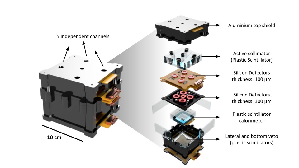
Layered structure of the LEM detector
Layered structure of the LEM detector
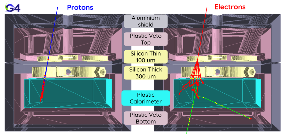
GEANT4-based simulation of the LEM detector response to incoming particles.
GEANT4-based simulation of the LEM detector response to incoming particles.
Lem specifications
| Feature | Silicon Detectors (PIPS) | Scintillator + SiPM |
|---|---|---|
| Energy Range | Low to Medium (0.1–20 MeV) | Medium to High (5–50 MeV) |
| Particle Types | Protons, Alphas, Electrons | Mainly Electrons |
| Resolution | High (~10%) | Moderate |
| Response Time | Moderate (ns–µs) | Fast (<1 ns) |
| Readout | Charge-sensitive preamps | Transimpedance preamps |
| Role | Spectroscopy | Timing, veto, calorimetry |
The LEM’s readout electronics were designed from the ground up to meet the challenging requirements of spaceborne low-energy particle spectroscopy, where high-resolution measurements, low noise, and low power consumption must coexist within strict constraints on size, redundancy, and thermal performance. At the core of the system lies a fully custom 16-channel, mixed-signal DAQ board, supported by dedicated preamplifiers for both silicon detectors and SiPMs, and orchestrated by a robust FPGA-based digital processing pipeline.
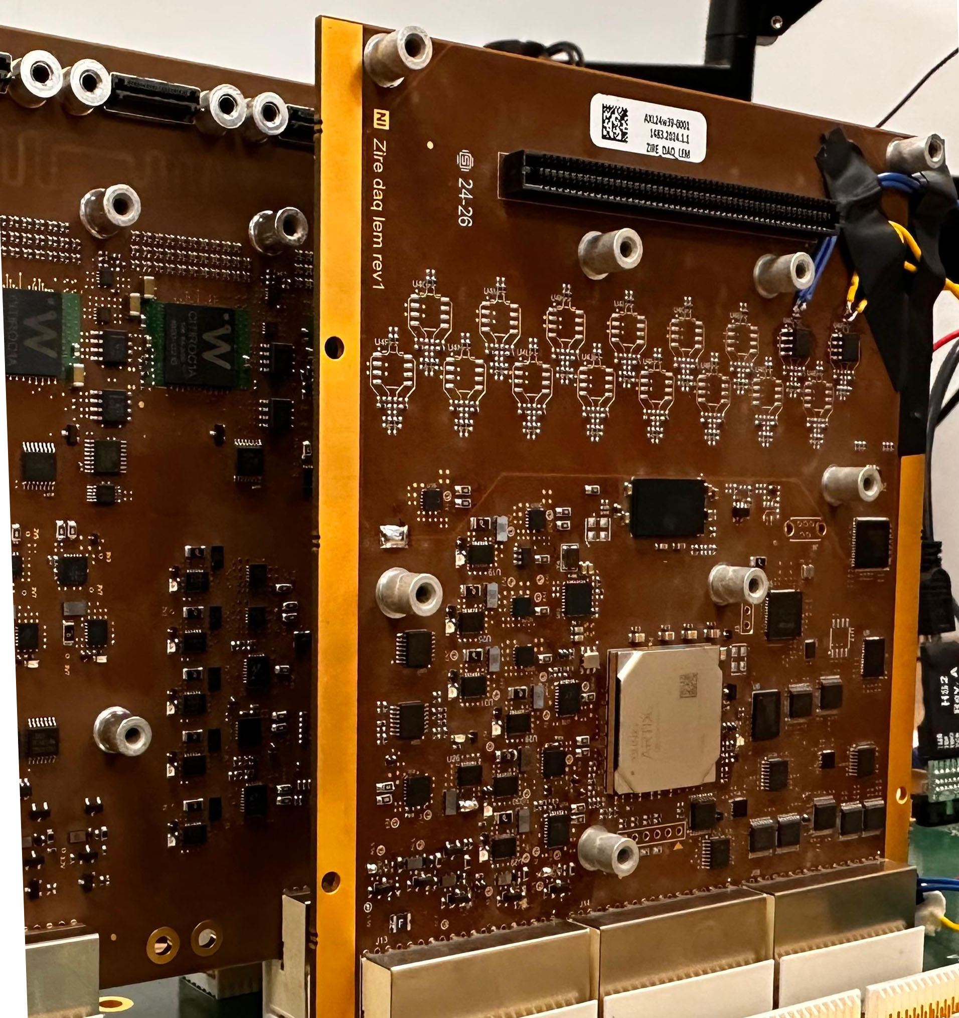
Photo of the LEM readout board
Photo of the LEM readout board

Block diagram of LEM DAQ board, showing ADC, FPGA, housekeeping components, and analog input sections.
Block diagram of LEM DAQ board, showing ADC, FPGA, housekeeping components, and analog input sections.
Analog Front-End: Dual Preamplifier Chains
The LEM detector employs two distinct analog front-end chains to optimally condition signals coming from the two sensor types:
Silicon Detector Preamplifier (High Gain)
Due to the relatively low intrinsic signal from silicon detectors, a high-gain, low-noise charge-sensitive preamplifier was designed in collaboration with AGE. This analog chain is optimized to:
- Preserve the signal shape over integration times in the range of 300 ns to 1 µs
- Provide sufficient gain and dynamic range for 10-bit ADCs
- Maintain low noise to ensure precise spectroscopy in the MeV range
This preamplifier has been tested in conjunction with a trapezoidal filter implemented in firmware to verify energy resolution under realistic conditions.
SiPM Preamplifier (Low Gain + HV Compensation)
The SiPM chain uses a transimpedance amplifier followed by a single-ended to differential converter, providing:
- Current-to-voltage conversion
- AC-coupling to isolate from HV bias offset
- Differential output for robust signal integrity
The input side is also designed to modulate the SiPM bias voltage using a low-side compensation loop driven by the DAQ board, enabling temperature compensation and gain stabilization in orbit.
The LEM DAQ Board
The main readout unit is a custom, compact DAQ board that integrates:
- ADC: Texas Instruments ADS52J90, 16 channels, 100 MSPS, 12-bit resolution, with LVDS output
- FPGA: Xilinx Artix-7 (same family as the FTK XU25P platform), handling all digital processing and trigger logic
- Housekeeping ADC: LTC2497 (16 channels) for thermal and voltage monitoring
- HV DAC: AD5391 for programmable SiPM bias control
- Pulser: Test signal generator for calibration and debug
- DC-DC converters, clock distribution, and USB interface for stand-alone testing
The DAQ board is housed within the electronics crate of the LEM and connects directly to the system backplane using the same mechanical and electrical form factor as the CITIROC-4 series. It operates at <6 W total power, thanks to the careful choice of low-power components and efficient data paths.
Data Pipeline and Digital Filtering
Inside the FPGA, a sophisticated processing chain implements:
- Trigger logic (based on silicon and SiPM coincidences)
- Trapezoidal energy filters (for MCA operation)
- Baseline restoration
- Pulse height and timing extraction
- Histogram accumulation (in high-rate mode)
- Scientific Data Packet Transmitter (SDPT) module for data transfer
The firmware also includes multiple diagnostic modules such as:
- Rate meters
- Temperature monitoring
- Timestamp generation (20 ns resolution)
- Slow control interface (SPI slave)
All signal processing is done digitally, enabling high flexibility, in-flight reconfigurability, and advanced data compression before downlink.
The firmware embedded in the LEM’s Artix-7 FPGA plays a central role in transforming raw analog signals into meaningful, physics-ready data products — in real-time, under tight constraints, and with the ability to adapt based on acquisition conditions. The firmware implements multiple modular processing blocks, each responsible for a critical stage of signal processing, triggering, event classification, or telemetry.
The LEM firmware is built around a real-time architecture that combines trigger logic, energy reconstruction, adaptive acquisition, and onboard data management. The trigger unit identifies valid events using programmable coincidence rules between silicon detectors and plastic scintillators, assigning each event to one of six physics-based classes with configurable prescaling. Energy processing is handled by a digital Multi-Channel Analyzer (MCA), which applies trapezoidal shaping to maximize signal-to-noise ratio, corrects baseline drifts, and extracts pulse height, time-over-threshold, and charge, while detecting pile-up and saturation. Depending on the incoming event rate, the system switches dynamically between List Mode, which records full-resolution events with timestamps and flags, and Histogram Mode, which compiles energy spectra per trigger class to reduce bandwidth usage during high flux periods. Data are formatted by the Scientific Data Packet Transmitter (SDPT) and sent via QSPI to the concentrator, with integrated modules for timestamping at 20 ns resolution, housekeeping (voltages, temperatures), rate diagnostics, and SPI-based slow control for configuration and health monitoring.

Modular firmware architecture showing data flow from trigger and MCA to SDPT and monitoring subsystems.
Modular firmware architecture showing data flow from trigger and MCA to SDPT and monitoring subsystems.
You may be interested in
Tags
External Links
- The Low Energy Module (LEM) of the Zire payload on board the NUSES space mission.
- A Compact Particle Detector for Space-Based Applications: Development of a Low-Energy Module (LEM) for the NUSES Space Mission
- The Ziré instrument onboard the NUSES space mission
- The Ziré instrument onboard the NUSES space mission - POSTER